
Products and Solutions
5G Transmit Chain
The 5G transmit chain is responsible for processing information bits by segmenting the data, adding Transport Block CRC and Code Block CRC, encoding the data with LDPC algorithm into code blocks (CBs), and interleaving the CBs based on control information governed by the 5G standard (3GPP TS 38.212).
For more information, please refer to the product brief, AR01B00V00.

For FPGA:
Clock frequency: 200MHz
Info bit throughput : 22.7Gb/s at rate 8/9
Latency : ~500 cycles
For ASIC*:
Clock frequency: 1GHz
Info bit throughput: 113Gb/s at rate 8/9
Latency : ~500 cycles
*Note: the above data are estimated.
LDPC Encoder Core
The LDPC Encoder Core encodes information bit sequences on the transmitting side using the LDPC algorithm. It is an optimal solution for shared channel coding in 5G NR applications. The core offers high operating speeds, a small hardware footprint, and superior efficiency. Furthermore, this design can be easily customized to support other standards, such as Wi-Fi or 6G. This implementation features a smaller silicon area and higher throughput than leading competing solutions. For higher-throughput applications like macro-cells, it can be configured to instantiate multiple cores.
For more information, please refer to the product brief, AR01B01V00.
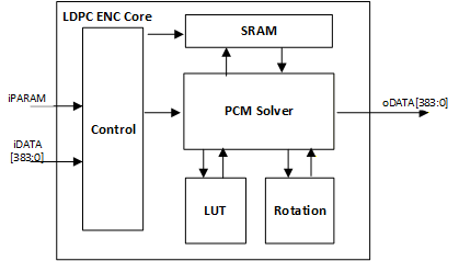
For FPGA:
Clock frequency at 270MHz
Coded throughput up to 18.5Gb/s
Latency : < 1.384us
Flop counts : 6381
LUT : 14k
BRAM : 5.5
For ASIC*:
Clock frequency at 1GHz
Coded throughput up to 68Gb/s
Latency : < 0.374us
Flop count: 7000
SRAM : 3.19KB
*Note: the above data are estimated.
CB Segmentation and TB/CB CRC Insertion
The module separates incoming information bits into code blocks (CB) and inserts Cyclic Redundancy Checks (CRCs) for each Transport Block (TB) and Code Block (CB) according to the 3GPP standard.
For more information, please refer to the product brief, AR01B05V00.

For FPGA:
Clock frequency: 300MHz
Max throughput: 42 Gb/s
Latency : 5 cycle
Resources: 1300 Flops, 3.4k LUTs
For ASIC*:
Clock frequency: 1GHz
Max Throughput: 120 Gb/s
Latency : 5 cycle
Resources: 1200 Flops
*Note: the above data are estimated.
Filler Insertion and Data Packing
The 5G NR standard defines a specific number of information bits for the LDPC encoder input. If the actual data size is smaller than this requirement, filler bits are appended to create a fixed-size information bit block, ensuring a uniform data width prior to encoding.
For more information, please refer to the product brief, AR01B02V00.

For FPGA:
Clock frequency: 330MHz
Max throughput: 42 Gb/s
Latency : 1 cycle
Resources: 600 Flops, 299 LUT
For ASIC*:
Clock frequency: 1GHz
Max Throughput: 128 Gb/s
Latency : 1 cycle
Resources: 600 Flops
*Note: the above data are estimated.
Filler & Parity Bits Removal and Data Packing
When performing LDPC encoding, filler bits may be added, and parity bits are generated and appended to the code block (CB). As specified by the 5G NR standard, the filler bits shall be removed, and extra parity bits shall be punctured before performing interleaving. The filler and parity removal module is designed to extract these bits from the encoded CBs, passing only the remaining information and parity bits to a downstream interleaver module for rate matching.
For more information, please refer to the product brief, AR01B03V00.
For FPGA:
Clock frequency: 285MHz
Max Throughput: 106Gb/s
Latency : 2 cycles
Resources:11,000 Flop, 13K LUTs
For ASIC*:
Clock frequency: 1GHz
Max throughput: 380Gb/s
Latency : 2 cycles
Resources : 6000 Flops
*Note: the above data are estimated.

Row-Column Interleaver
A row-column interleaver is a digital signal processing technique used to combat transmission burst errors. As specified by the 5G NR standard (3GPP TS 38.212), it restructures data sequences without changing the original information by writing encoded bits into a matrix row by row and reading them out column by column. Compared to a leading competing solution, this implementation cuts silicon area in half and triples data throughput.
For more information, please refer to the product brief, AR01B04V00.
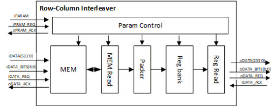
For FPGA:
Clock frequency at 250MHz
Max throughput: 32 Gb/s
Latency : 6 cycles
Resources : 15,722 Flops, 25,891 LUTs
For ASIC*:
Clock frequency: 1GHz
Max Throughput: 128Gb/s
Latency : 6 cycles
Flop count: 15,700
*Note: the above data are estimated.